Through the years, IQE has been instrumental in numerous collaborations and programs aimed at leveraging the advantages of advanced compound semiconductors to compliment traditional silicon-based technology.
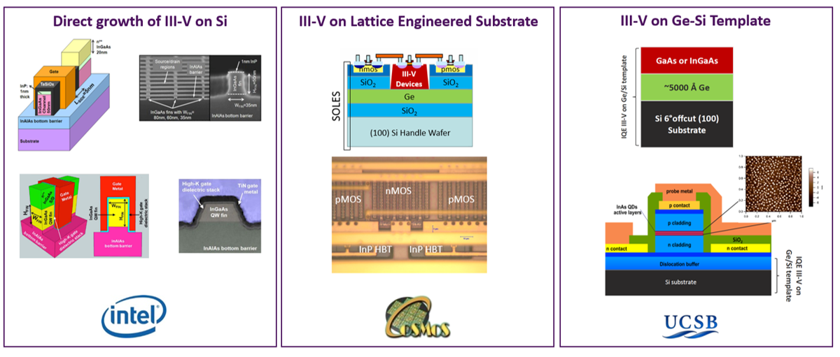
These efforts provide a practical path for the realisation of compound semiconductors on larger form factor wafers (>=200 mm), thereby enabling III-V materials to be integrated with leading edge CMOS technology. Referred to as heterointegration, these efforts have spanned a variety of markets (e.g., advanced RF, electronics, and photonics). IQE is a leader in multiple technologies for the growth of III-V on silicon.
III-V on Si: Three approaches to Heterointegration
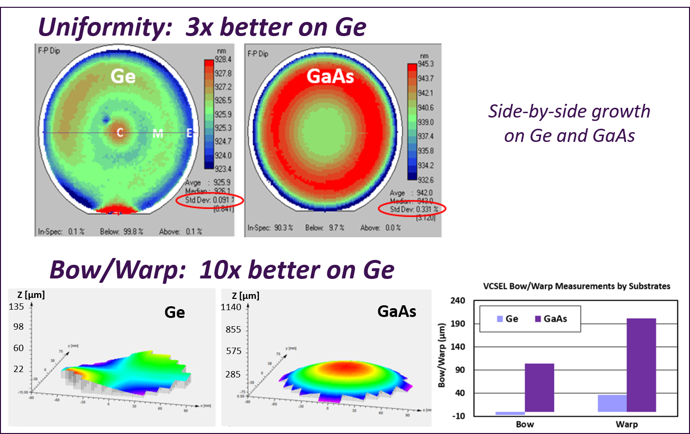
IQE has used its expertise in this area to develop a technology for VCSEL epi growth on Germanium substrates (IQGeVCSEL 150TM). This provides VCSEL wafers with reduced defectivity, reduced wafer bow/warp, and improved uniformity. In addition, this provides a viable route to realising VCSELs on larger form factor wafers (Ge is commercially available on diameters up to 200 mm). Ultimately, this technology can be combined with IQE’s world leading Ge/Si template technology (TDD < 1E6 cm-2) to provide the ultimate integrated solution. Although recent efforts have focused on VCSEL epiwafers, this technology can be readily applied to all III-V materials and wafer types.
Data for IQGeVCSEL 150™